My son has been doing a lot of digging in the board and finally we found that the SRAM chip had a faulty bit (bit 3 was always low) so anything that used RAM was corrupted. After a quick circuit change we got the board working as a whole. He emediately started working on BIOS routines and a SREC parses, to enable us to actually load code in the RAM and run it from the console. That will be nice!
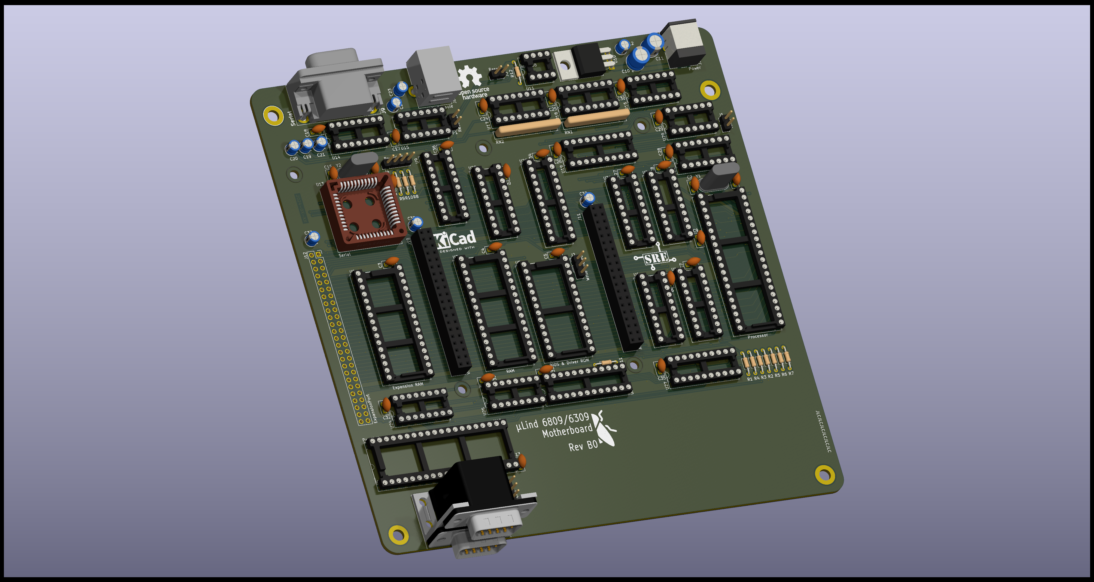
He came back to me and asked that we integrate a read back function to the bank register, it was write only in the design, and said that he could make the memory management a lot better if he could read what the banks where configured as. Since i was finished with the routing of the stage 2 board (I just wanted to test some of the stage 2 features on the stage 1 board before ordering) I just sighed and started drawing. It was not a big change, just a new buffer chip, but it required a lot of re-wireing to be able to get the signals correct.
But it is done! 
We also removed the reset signal to the USB chip, letting us keep the serial connection during a reset. It is implemented with a jumper so if things need to be resetted we can jumper it back.
So now I need to try all stage 2 features I have prototype boards for (the 6522 joy-port, the complete address decoder and the interrupt handler) so I can order stage 2!

